
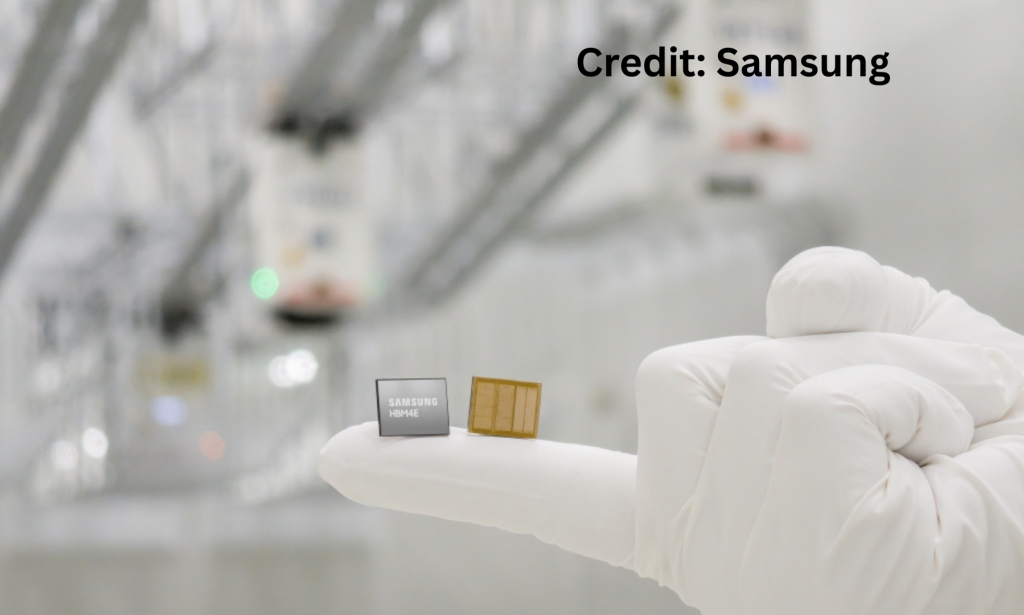
Samsung Electronics has just taken another major step in the AI memory race. The company today announced it has begun shipping the world's first 12-layer HBM4E samples to major global customers making it the first in the industry to reach this milestone and further extending its lead in next-generation High Bandwidth Memory technology.
What Is HBM4E and Why Does It Matter?
HBM4E is the enhanced version of Samsung's HBM4 memory, designed specifically to handle the most demanding AI workloads of the next generation. As large language models grow larger, AI training clusters consume more memory bandwidth than ever before, and HBM4E is built to meet those demands at a scale that previous generations simply cannot match.
This announcement comes just months after Samsung became the first company in the world to begin mass production and commercial shipment of HBM4 earlier in 2026, meaning the company has now moved from HBM4 mass production directly into HBM4E sample shipments without pause.
Speed and Bandwidth, The Core Performance Numbers
Samsung's HBM4E delivers a stable pin speed of 14 gigabits per second (Gbps), with the ability to scale up to 16Gbps under demanding conditions. That represents more than a 20% speed improvement over HBM4. Combined with a memory bandwidth of up to 3.6 terabytes per second (TB/s) per stack, HBM4E is built to keep the most powerful AI accelerators and data center processors fed with data at a rate that maximizes their computing potential for large language models and next-generation AI systems.
48GB Capacity With Room to Grow
The initial 12-layer HBM4E sample ships in a 48GB configuration more than 30% capacity increase over the previous generation. Samsung has also confirmed plans to expand the lineup to include a 32GB 8-layer variant and a 64GB 16-layer variant, giving customers flexibility to choose the configuration that best fits their specific AI infrastructure requirements.
What Technology Powers HBM4E
Samsung's HBM4E is built on the company's most advanced 6th-generation 10nm-class DRAM process, known internally as 1c, alongside Samsung Foundry's 4nm logic base die. This same combination of core and base die technology was refined through the company's HBM4 production experience, giving HBM4E a level of process stability and manufacturability that a brand-new architecture would not have.
Design and process optimization across both the memory and logic layers has delivered meaningful gains across three key areas. Energy efficiency improved by 16% compared to HBM4. Thermal resistance characteristics improved by more than 14%, meaning the memory dissipates heat more effectively critical requirement for AI data centers running sustained, intensive workloads around the clock. These thermal improvements also translate directly into longer-term reliability and lower energy bills at scale.
Samsung's Competitive Position in HBM
The HBM market has become one of the most strategically important battlegrounds in the global semiconductor industry, driven almost entirely by the explosion in AI infrastructure spending. Samsung's ability to ship HBM4E samples at this stage is significant because it keeps the company at the front of the technology roadmap at a time when AI chip customers are already planning their next hardware generations.
Sang Joon Hwang, Executive Vice President and Head of Memory Development at Samsung Electronics, stated that following the successful mass production of HBM4, Samsung has again demonstrated its distinct technological edge by moving into HBM4E, and that through its advanced manufacturing capabilities and preemptive infrastructure investments, it will continue to drive the growth of the global AI memory market.
Customer feedback on HBM4, which entered mass production in February 2026, has been strongly positive particularly around performance and energy efficiency. With HBM4E using the same proven core and base die combination as HBM4, Samsung anticipates a smooth transition into HBM4E mass production aligned with customer schedules following the current sample phase.
The Bigger Picture Samsung's Full-Stack AI Memory Strategy
What makes Samsung's position in HBM unique is the breadth of its in-house capabilities. Unlike most competitors, Samsung controls the full semiconductor supply chain for HBM memory design, DRAM process technology, logic base die through Samsung Foundry, and advanced packaging. This vertical integration allows Samsung to optimize every layer of the HBM stack together rather than relying on external partners for any part of the process, which gives it both a performance and a time-to-market advantage.
As AI data center spending continues to accelerate globally and the demand for High Bandwidth Memory remains tightly supply-constrained, Samsung's early position in HBM4E puts it in a strong place to capture a significant share of the next wave of AI chip orders from hyperscale customers around the world.

You must be logged in to post a comment.